Research Projects
Our research investigates quantum transport and coherent phenomena in low-dimensional systems based on 2D materials and semiconductor platforms. We focus on spin and valley physics in quantum dot systems, superconducting hybrid devices, and microwave circuit quantum electrodynamics as complementary approaches to probing and controlling quantum states. An overview of our research is given below.
Electrostatically defined nanodevices in bilayer graphene
(Artem Denisov, Christoph Adam, Jonas Gerber, Lara Ostertag, Jessica Richter, Clara Galante, Tijl Degroote, Clara Scherm)
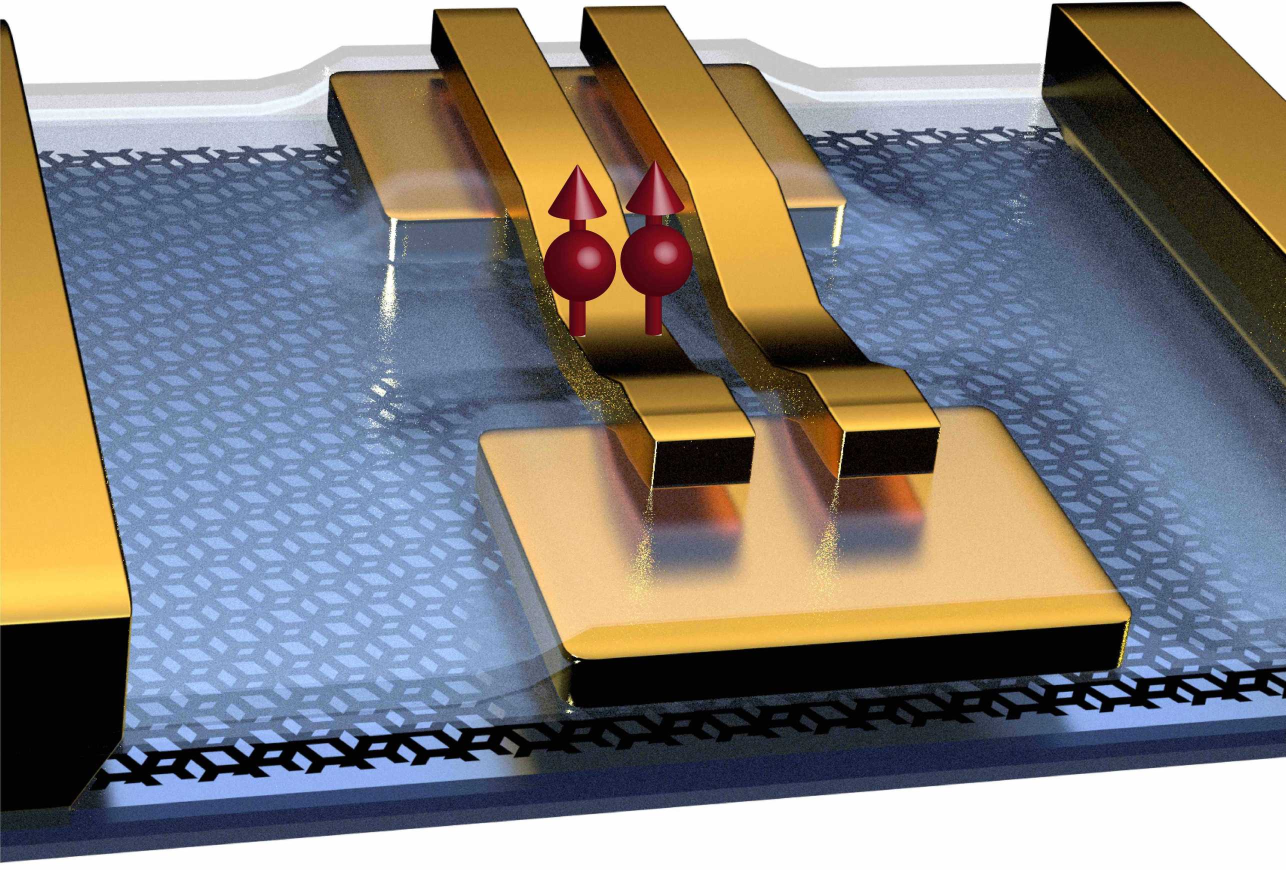
We explore bilayer graphene as a potential platform for spin qubits. Its low atomic mass and the low natural abundance of nuclear spins result in weak spin–orbit coupling and minimal hyperfine interaction. These are key ingredients for achieving long quantum coherence times.
A central advantage of bilayer graphene is its electrically tunable band structure. Applying a perpendicular displacement field opens a bandgap in the otherwise gapless material, enabling electrostatic confinement of charge carriers. Using top- and back-gate electrodes, we define gate-controlled quantum dots with high tunability [1,2]. To probe these devices, we employ capacitive coupling to on-chip charge detectors, allowing real-time detection of single-electron occupation [3]. This approach provides detailed access to the quantum dot energy spectrum [5] and enables advanced thermodynamic measurements, including entropy [4].
We further investigate spin and valley dynamics by measuring relaxation times (T₁) in single [6] and double quantum dots [7]. We observe spin–valley relaxation times exceeding 30 seconds [8], highlighting the potential of bilayer graphene for robust and long-lived qubit implementations.
References:
[1] C. Tong, et al., Phys. Rev. Lett. 133, 017001 (2024)
[2] C. Tong, et al., Phys. Rev. Res. 6, L012006 (2024)
[3] R. Garreis, et al., Phys. Rev. Res. 5, 013042 (2023)
[4] C. Adam, et al., Phys. Rev. Lett. 135, 126202 (2025)
[5] H. Duprez, et al., Nat. Commun. 15, 9717 (2024)
[6] L. M. Gächter, R. Garreis, et al., PRX Quantum 3, 020343 (2022)
[7] R. Garreis, C. Tong, et al., Nat. Phys. 20, 428 (2024)
[8] A. O. Denisov, et al., Nat. Nanotechnol. 20, 494 (2025)
Electronic properties of transition metal dichalcogenides (TMDs)
(Jonas Gerber, Markus Niese, Tijl Degroote, Joshua Williams)
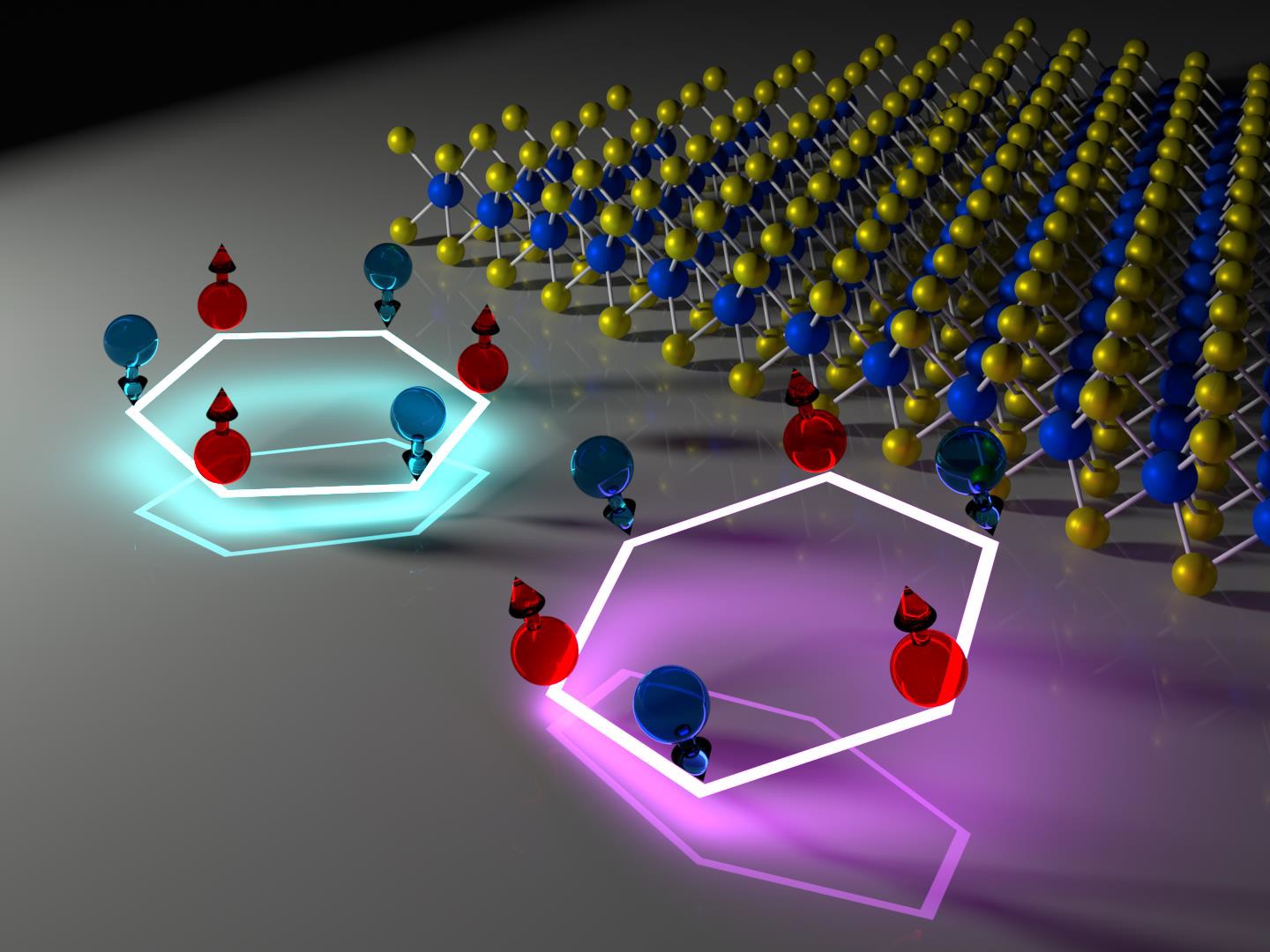
We investigate transition metal dichalcogenides (TMDs) and their integration into van der Waals heterostructures as a platform for engineered quantum devices. Semiconducting TMDs such as MoS₂ and WSe₂ provide access to a wide range of electronic regimes, while their combination with graphene enables tailored proximity effects and novel functionalities.
In TMD materials, we study the electronic band structure using magnetotransport experiments [1,2].Their sizable band gaps (≈1–2 eV) allow for robust electrostatic confinement, which we exploit to realize gate-defined nanostructures, including quantum point contacts [3] and quantum dots [4].
Beyond individual materials, a central focus of our work is on hybrid devices combining TMDs with graphene, in particular bilayer graphene. In these heterostructures, proximity-induced spin–orbit interaction enables control over spin and valley degrees of freedom, opening new routes toward spin-based quantum devices [5].
Building on these capabilities, we aim to realize and study superconducting hybrid structures in TMD-based heterostructures, motivated by recent observations of superconductivity in related systems. Such platforms provide a promising route toward combining strong spin–orbit coupling, gate tunability, and superconducting correlations within a single device architecture.
References:
[1] M. Masseroni, et al., Phys. Rev. Lett. 3, 023047 (2021)
[2] M. Masseroini, et al., Nano Lett. 25, 26, 10472 (2025)
[3] R. Pisoni, et al., Nano Lett. 17, 8, 5008 (2017)
[4] R. Pisoni, et al., Appl. Phys. Lett. 112, 123101 (2018)
[5] J. Gerber, et al., Nano Lett. 25, 33, 12480 (2025)
Twisted graphene-based nanodevices
(Marta Perego, Alexandra Mestre-Torà)
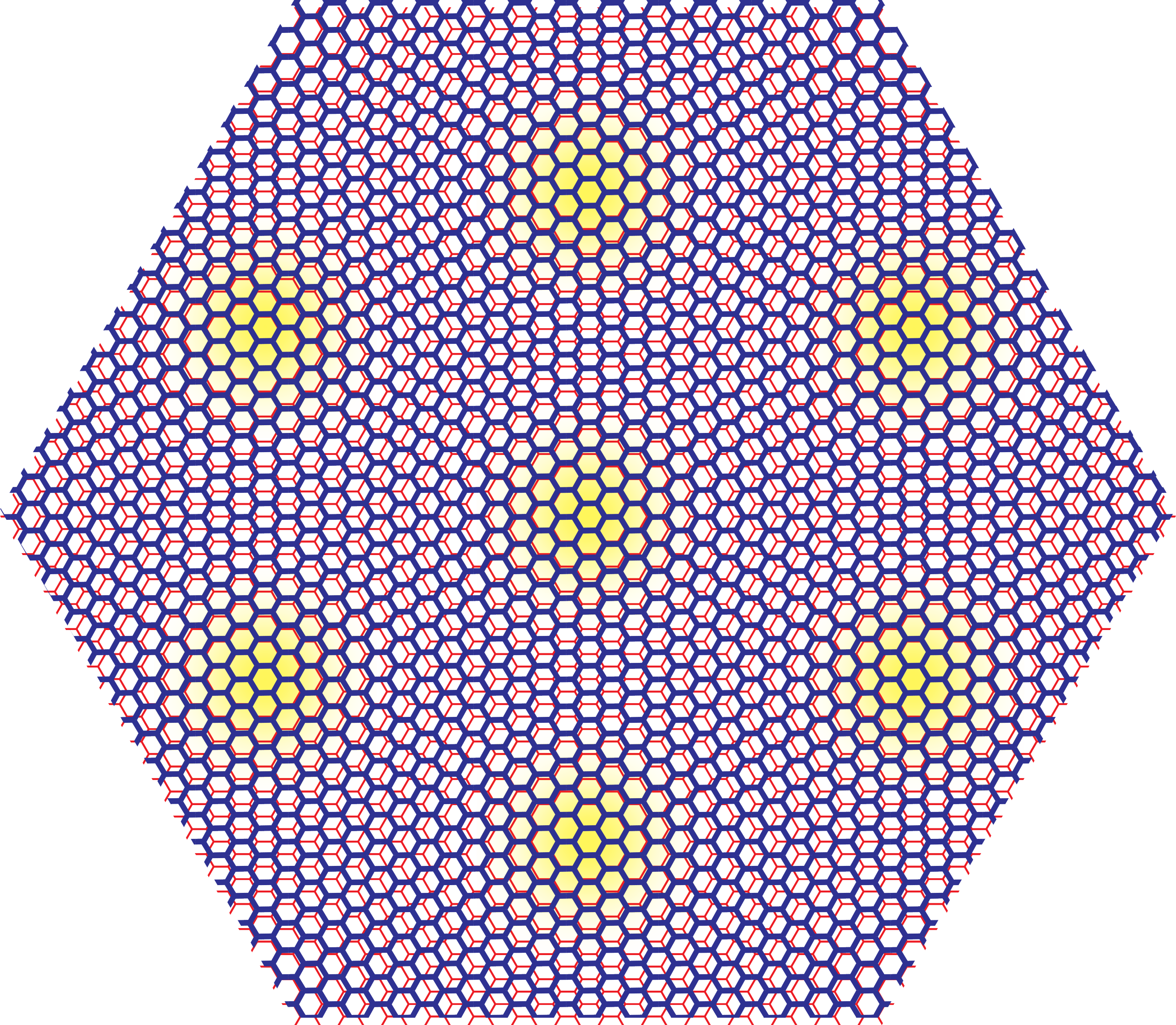
We investigate twisted graphene systems, in particular magic-angle twisted bilayer graphene (MATBG), as a platform for strongly correlated and superconducting quantum matter. Moiré superlattices enable the emergence of insulating, magnetic, and superconducting phases within a single device, offering exceptional tunability of electronic states.
Using multilayer gate architectures, we achieve local electrostatic control of these phases and realize fully gate-defined nanodevices in a correlated material [1]. A central focus of our work is the development of superconducting hybrid structures based on MATBG. We have demonstrated gate-defined Josephson junctions exhibiting both DC and AC Josephson effects [1], and engineered devices with tunable junction geometry, enabling controlled weak links and superconducting constrictions [2].
Building on this level of control, we realize complex device architectures such as monolithic, gate-tunable SQUIDs [3] and ring geometries to probe quantum coherence. In these systems, we observe interference phenomena including the Aharonov–Bohm effect in the normal state and the Little–Parks effect in the superconducting regime [4].
Our devices further provide access to key properties of the superconducting state. From transport through gate-defined Josephson junctions, we extract quantities such as superfluid stiffness and electron–phonon coupling [5].
In addition, we investigate vortex physics in twisted graphene, revealing signatures of vortex dynamics and spontaneous vortex penetration through field-dependent critical currents and bistable switching behavior [6,7].
References:
[1] F. K. de Vries, et al., Nat. Nanotechnol. 16, 760 (2021)
[2] G. Zheng, et al., Phys. Rev. Res. 6, L0112051 (2022)
[3] E. Portolés, et al., Nat. Nanotechnol. 17, 1159 (2022)
[4] S. Iwakiri, et al., Nat. Commun. 15, 390 (2024)
[5] E. Portolés, et al., Nat. Commun. 16, 4273 (2025)
[6] M. Perego, et al., Nat. Commun. 16, 10259 (2025)
[7] M. Perego, et al., arXiv:2601.21735 (2026)
Superconducting-semiconductor hybrid devices
(Artem Denisov, Clara Galante, Aaron Anhalt)
We develop and apply complementary microwave and DC techniques to probe and control quantum states in semiconductor and van der Waals nanostructures. These approaches form a unifying methodological framework across our research on graphene-, TMD-, silicon-, and germanium-based devices, enabling both coherent spectroscopy and transport studies of quantum coherence, spin, and superconducting correlations in engineered nanosystems.
A central tool is circuit quantum electrodynamics (cQED), where superconducting microwave resonators are capacitively coupled to gate-defined nanodevices. This enables coherent interaction between microwave photons and electronic degrees of freedom in quantum dots and related structures. In early experiments, performed in collaboration with the Wallraff group, we demonstrated strong coupling between double quantum dot charge qubits and single microwave photons using high-impedance resonators, which enhance light–matter coupling by an order of magnitude compared to standard 50 Ω designs [1]. These techniques established superconducting resonators as a powerful probe of semiconductor qubits.
Building on this platform, we achieved strong spin–photon coupling using resonant exchange spin qubits, where spin states are hybridized with charge degrees of freedom to enhance microwave coupling [2]. This was extended to coherent coupling between multiple qubit implementations, including charge–charge, charge–transmon, and spin–transmon systems [3–5], as well as more complex gate-defined triple quantum dot configurations [6].
In ongoing work, we are transferring this circuit QED toolbox to graphene-based quantum dots [7,8], motivated by their long coherence prospects and spin–valley physics, with the aim of reaching the strong coupling regime between 2D material qubits and microwave resonators.
In parallel, we investigate superconducting hybrid nanostructures using DC transport techniques. These devices, based on graphene, TMDs, and related van der Waals materials, enable controlled studies of proximity-induced superconductivity, Andreev reflection, and Josephson physics in mesoscopic systems. Superconducting correlations are engineered via coupling to conventional superconductors such as aluminum or intrinsically superconducting 2D materials including NbSe₂, allowing systematic exploration of superconducting order in low-dimensional and gate-tunable environments.
This direction directly connects to our work on superconducting graphene- and TMD-based devices described above. A key objective is to unify these approaches: combining microwave resonator-based circuit QED with DC-defined superconducting hybrid devices. Such integrated architectures would enable simultaneous coherent spectroscopy and transport control, providing a versatile platform for studying quantum coherence, correlated electron states, and hybrid qubit concepts in engineered nanoscale systems.

References:
[1] A. Stocklauser, et al., PRX 7, 011030 (2017)
[2] A. J. Landig, et al., Nature 560, 179 (2018)
[3] D. J. van Woerkom, et al., PRX 8, 041018 (2018)
[4] P. Scarlino, et al., Nat. Commun. 10, 3011 (2019)
[5] A. J. Landig, et al., Nat. Commun. 10, 5037 (2019)
[6] J. V. Koski, et al., Nat. Phys. 16, 642 (2020)
[7] M. J. Ruckriegel, et al., Nano Lett. 24, 7508 (2024)
[8] M. J. Ruckriegel, et al., arXiv.2511.20185 (2025)
Silicon and Germanium devices for spin qubit applications
(Petar Tomić, Yuze Wu, Patrick Bütler)
We investigate spin qubits in semiconductor nanostructures based on silicon and germanium, leveraging their compatibility with scalable fabrication technologies and their suitability for long-lived quantum states. Our work focuses on understanding and engineering the electronic and noise environments that govern qubit coherence and control.
A major part of our research addresses spin qubits in industrial silicon MOS devices, fabricated in 300 mm CMOS pilot lines at Imec. These systems provide a platform to study the impact of realistic device disorder and noise on qubit performance. We investigate strategies to mitigate decoherence by tailoring qubit encoding to the spatial structure of the noise environment. Using this approach, we have demonstrated significantly enhanced coherence times, reaching millisecond-scale Hahn-echo coherence [1].
In parallel, we study hole-based spin qubits in planar Ge/SiGe heterostructures, which combine high mobility, low effective mass, and strong spin–orbit coupling. These properties enable fast, all-electrical qubit control without the need for additional micromagnets, while maintaining compatibility with scalable device architectures. We investigate quantum transport in gate-defined single and double quantum dots formed in high-mobility Ge/SiGe quantum wells.
Beyond planar heterostructures, we also explore germanium MOS devices to assess their potential for spin-based quantum technologies. Across these platforms, our goal is to understand hole and electron transport in realistic device environments and to advance semiconductor-based architectures for scalable quantum information processing.
References:
[1] P. Tomić, et al., arXiv:2512.20758 (2025)